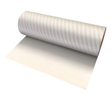
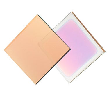
Fundamentals of Anisotropic Conductive Film (ACF)

Dexerials Corporation is a materials manufacturer specializing in functional materials and electronic components. Guided by their corporate vision, “Value Matters: Creating what never existed before. Creating value for the world,” they are actively expanding their product offerings beyond their traditional electronics field into the automotive industry, environmental solutions, and life sciences.


“Tech Times” is a site that clearly conveys fundamental knowledge on adhesion, bonding, thermal conductivity, optical design, and more to engineers across various fields. Dexcerials, with years of experience manufacturing and selling electronic components, bonding materials, optical materials, and more, leverages its accumulated expertise to provide support that resolves the challenges faced by engineers.
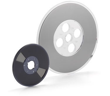
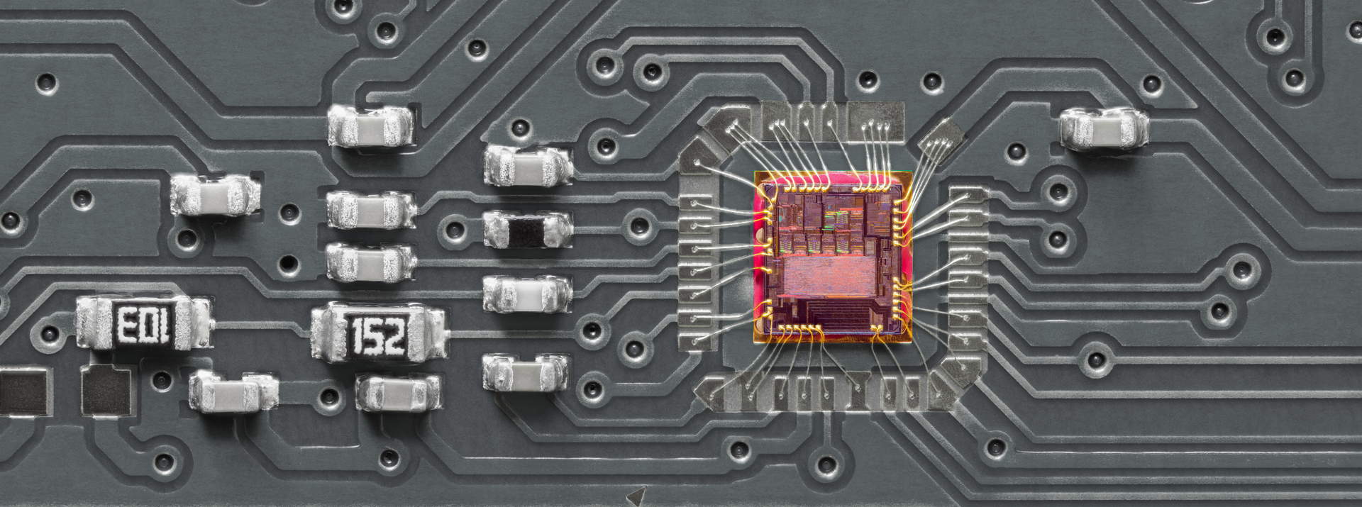
Contributes to device thinning and miniaturization. Achieves excellent connection reliability.
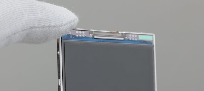
A film-type bonding material that disperses conductive particles within a resin, combining conductive and insulating properties. Used for connecting substrates in displays, camera modules, and other applications.
ACF for Chip On Glass in Medium/Small FPDs
ACF for Film On Glass in Medium/Small FPDs
ACF for Film On Glass for Large FPDs
ACF for Film On Glass for Large FPDs
ACF for Film On Board for Automotive Applications
ACF for IC Cards
ACF for Film On Board/Film Applications Replacing Solder and Connectors
ACF for Film On Glass Applications for Glass Touch Panels
Film On Plastics for Film Touch Panels
Fundamentals of Anisotropic Conductive Film (ACF)
New Applications for Anisotropic Conductive Film (ACF)
Smartphone/Tablet PC Cameras, In-Vehicle Cameras, Security Cameras

Benefits of Biometric IC Credit Cards - Diversifying Payment Methods
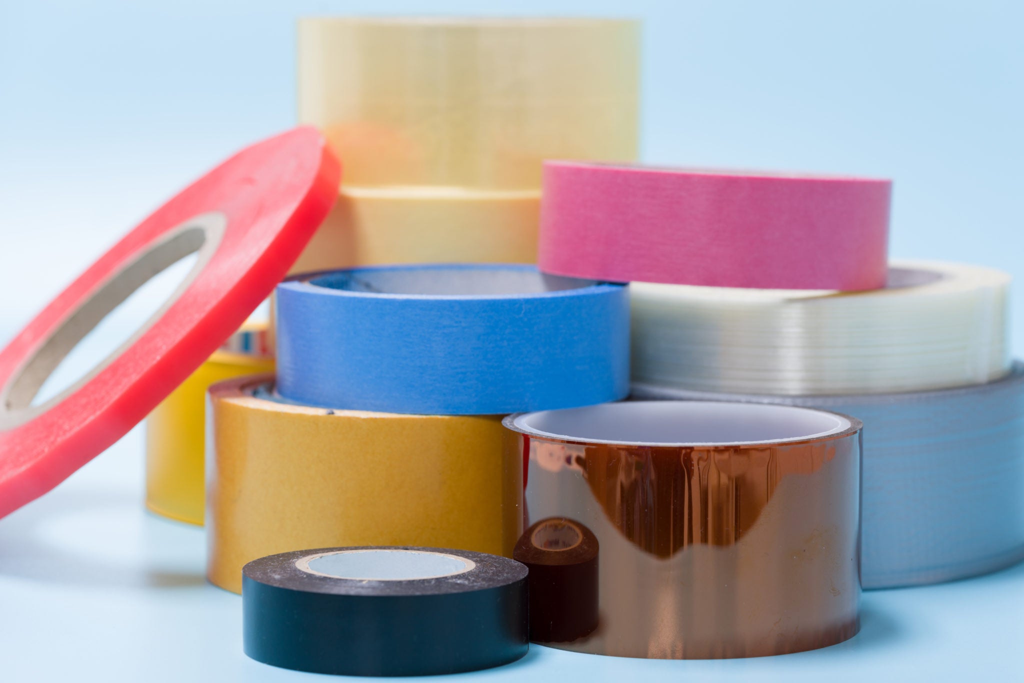
Foundational Products Supporting Bonding in Electronics
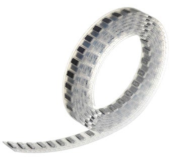
Industrial double-sided tapes ranging from general-purpose adhesive types to thermosetting types, selectable according to application. Their lineup includes products with added functionalities tailored to specific applications. They also pursue ease of use in various aspects, such as die-cutting performance and reworkability.
General-Purpose Double-Sided Adhesive Tape
Special Resin-Based Heat-Activated Adhesive Tape
Bonding Sheets for FPCs
Low Outgassing Double-Sided Adhesive Tape
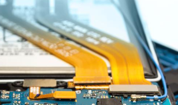
Fundamentals of Flexible Printed Circuits (FPC)
and Their Manufacturing Technology

Evaluation Methods for Functional Tapes
Fundamentals of “Adhesion”
- Learning from Adhesive Tape Technology
Tape Products for Protecting and Adding Functionality to Electronics
Industrial single-sided tapes designed to protect or add functionality to electronics and their manufacturing processes. Their lineup includes PET-based single-sided tapes for temporary fixing and specialty single-sided tapes with specialized substrates for adding functions like EMI shielding.
Removable Tape
Adhesive-Backed Dust Covers for Speakers
Conductive Single-Sided Adhesive Tape for Shielding
Fundamentals of Flexible Printed Circuits (FPC)
and Their Manufacturing Technology
Evaluation Methods for Functional Tapes
Fundamentals of “Adhesion”
-Learning from Adhesive Tape Technology
Lineup for securing electronic components with excellent electrical insulation and fixing precision parts
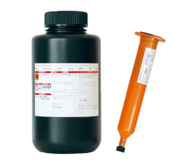
Industrial adhesives providing bonding functions tailored to specific applications. They meet diverse needs arising from the miniaturization and high performance of electronic devices by adding features such as electrical insulation, self-extinguishing properties, and short-term bonding.
Silicone Rubber-Based Self-Extinguishing Adhesives
Polyester Resin-Based Self-Extinguishing Adhesives
UV-Curable Adhesives
Dual-Cure UV/Heat-Curable Adhesives
Thermosetting Adhesive
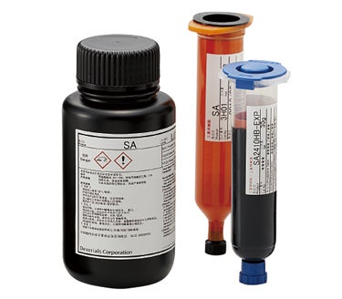
Anisotropic Conductive Paste (ACP)

How to Use Industrial Adhesives

Technology of Epoxy Adhesives Curing with UV or Heat

Mechanism of Thermosetting Adhesives (Crosslinking Reactions and Their Types)
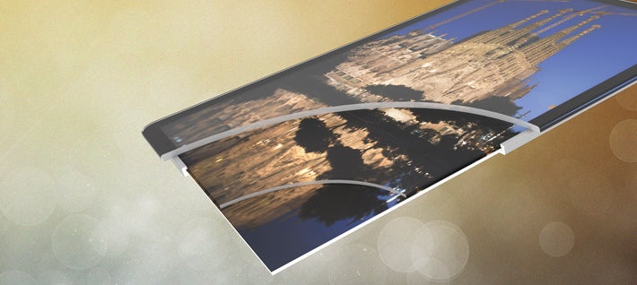
From light-manipulating resin to more beautiful displays
Achieves enhanced display visibility and slim profiles by filling the air gap inside displays—such as those in smartphones, tablet PCs, notebook PCs, and in-vehicle navigation systems—with a highly light-transmissive UV-curable elastic resin.
SVR for Medium/Small FPDs
Hybrid Type SVR for Medium/Small FPDs

Excellent Properties and Features of Optical Clear Resins

Diverse Optical Laminating Processes for Optical Clear Resins
Basic Knowledge of Optical Clear Resins
Achieving Displays Visible Indoors and Outdoors
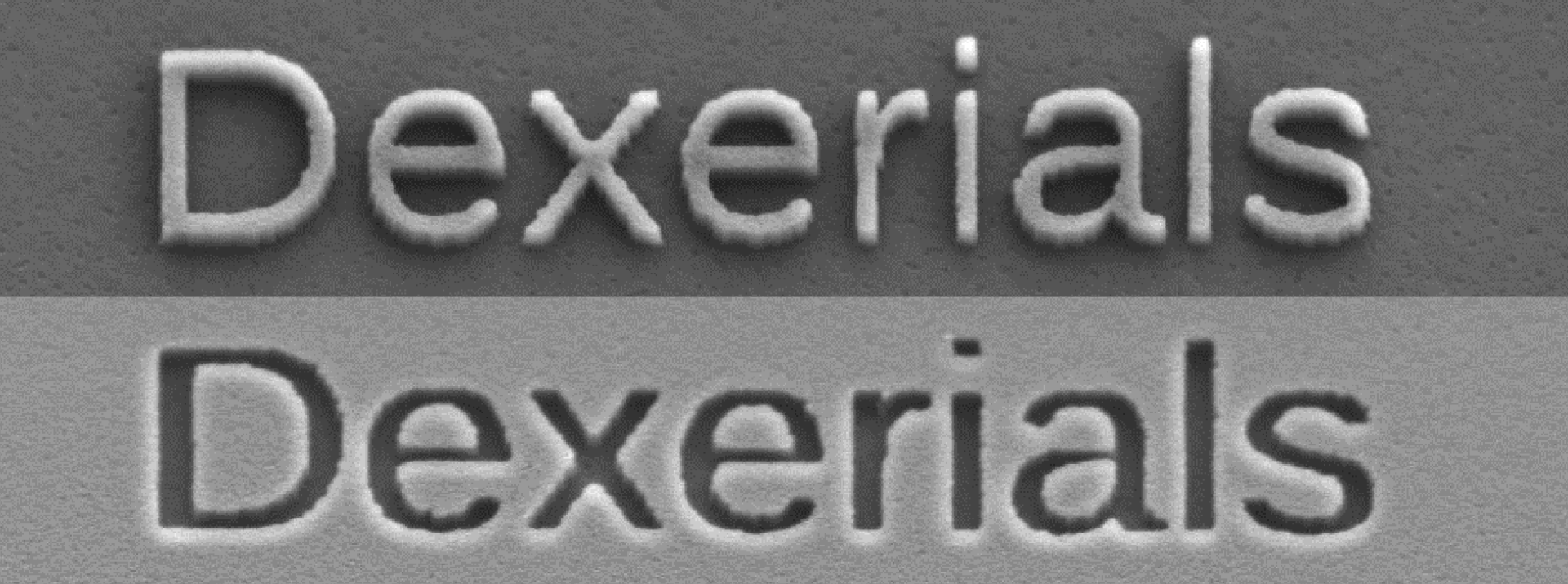
Utilizing a patterning method capable of controlling film thickness at the nanometer level, it incorporates an anti-reflective coating composed of multiple layers with differing refractive indices within its structure. This coating utilizes light interference to reduce reflected light. It also offers high practicality, such as being suitable for use on touch panel surfaces, because of its excellent anti-soiling properties and scratch resistance./p>
Anti-Reflective Film
Learn more about this product here ->
Moss Eye Type Anti-Reflective Film

Enhancing Automotive Luxury with “Piano Black”: New Anti-Reflective Film Technology

Anti-Reflective Film Using Roll-to-Roll Sputtering Technology

Fundamentals of Anti-Reflection Using Optical Thin Films
Optical Devices Supporting High-Brightness Projection
This optical device utilizes nanoscale process technology to form high-quality optical control structures on its substrate surface. By leveraging its substrate's inherent properties, it achieves high heat resistance, light resistance, and durability, contributing to the high brightness and high contrast of projectors.
Inorganic Waveplates (1/4-wave, 1/2-wave, etc.)
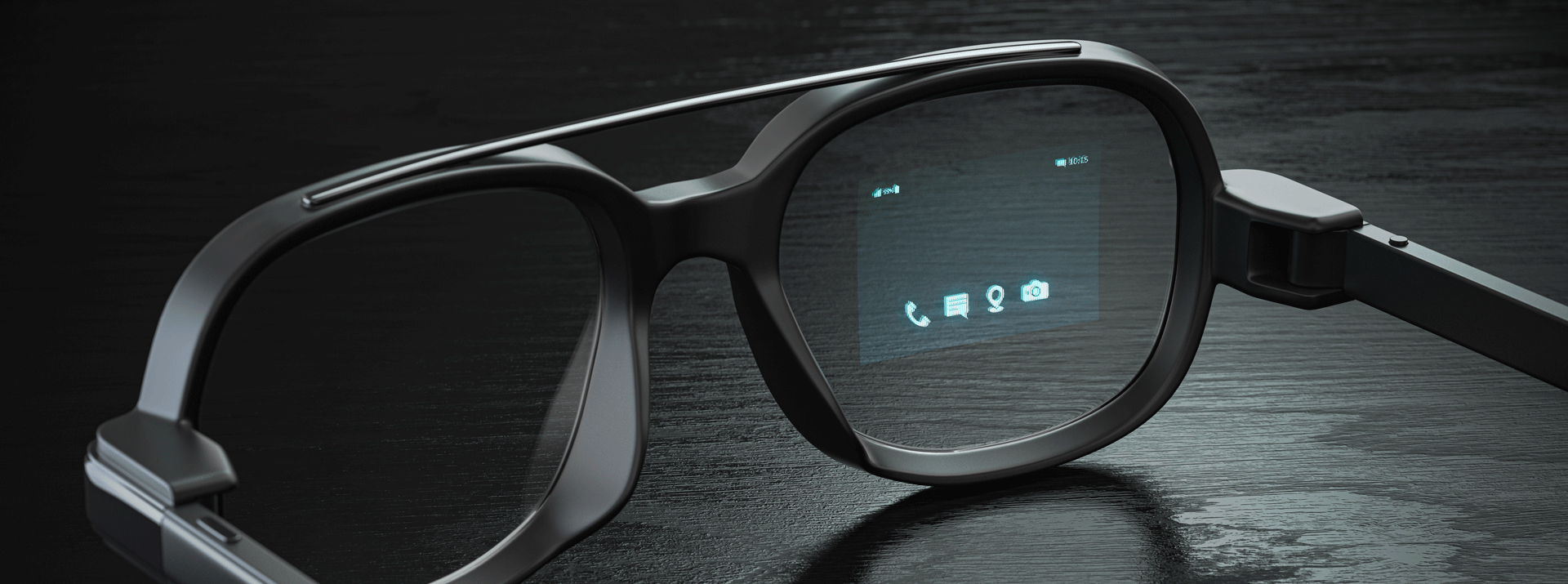
AR/VR Device Trends and Challenges
——Technologies and Products as Solutions

Inorganic Polarizers --Their Technology and Features

How to Further Enhance Projector Brightness and Durability? Features of Inorganic Optical Devices
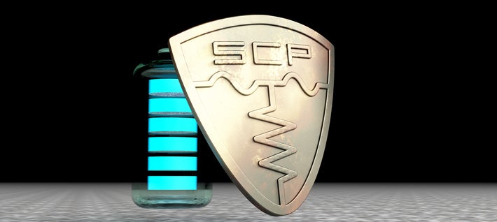
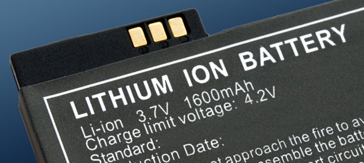
Protecting Lithium-ion Batteries
This surface-mount fuse reliably interrupts overcharging and overcurrent in lithium-ion batteries. The Self-Control Protector (SCP) handles both overcurrent and overvoltage. The Power Current Protector (PCP) is optimized for high-current applications by addressing overcurrent only, it maintains the same compact package as the SCP.
150A SFM Series Self-Controlled Protector (SCP)
120A SFM Series Self-Controlling Protector (SCP)
60A SFK Series Self-Controlled Protector (SCP)
45A SFK Series Self-Control Protector (SCP)
30A (Compact) SFS Series Self-Control Protector (SCP)
30A (Compact) SFH Series Self-Control Protector (SCP)
30A SFK Series Self-Control Protector(SCP)
22A(小型) SFJ Series Self-Control Protector(SCP)
15A(小型) SFJ Series Self-Control Protector(SCP)
12A(小型・薄型) SFR Series Self-Control Protector(SCP)
12A(小型) SFJ Series Self-Control Protector(SCP)
5A(小型・薄型) SFR Series Self-Control Protector(SCP)
100A PTA Series パワーカレントプロテクター(PCP)
65A PSK Series パワーカレントプロテクター(PCP)
35A PSH Series パワーカレントプロテクター(PCP)
Learn more about this product here ->
Secondary Protection Circuits for Lithium-Ion Batteries: The Function and Evolution of Fuse Elements
Why Do Lithium-Ion Batteries Need Secondary Protection Elements? Preparing for Overcurrent and Overcharging

The Global Spread of “Electric Motorcycles” and Their Safety (Batteries and Secondary Protection Fuses)
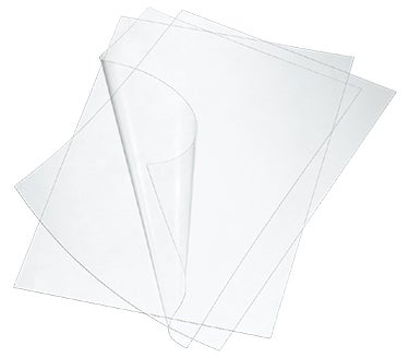
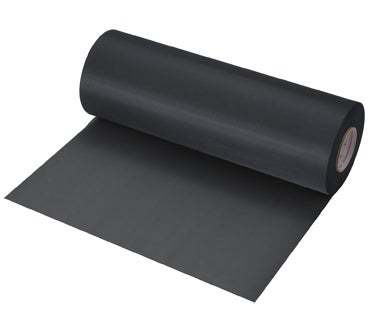
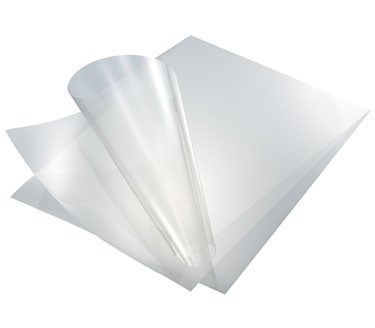
Low-Reflection, High-Transmittance Film Utilizing a Moss Eye Structure
This high-transparency film boasts a transmittance rate of over 98%. By forming nano-level microstructures mimicking the structure of a moth's eye on both sides of the base film, it eliminates refractive index differences, achieving low reflection and high transmittance. It provides a clear, natural view as if nothing were obstructing it. Suitable for eye shields and face shields, it reduces eye fatigue even during prolonged wear.
DexShield

Features of Medical Shield Materials Utilizing Anti-Reflective Film (Moth Eye Type)

What is the Moth Eye Structure? - In Pursuit of Ultimate Anti-Reflection -
The Journey to Creating an Ultra-Transparent Anti-Reflective Film You Won't Even Notice - The Latest Technology for Forming Microstructures –
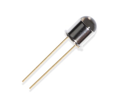
Semiconductor devices utilizing the mechanism of converting electric current into light
LEDs (light-emitting diodes) are semiconductor devices that convert electrical current into light. The color (wavelength) emitted is determined by the materials used in their construction. We handle LEDs across a wide spectrum of colors (wavelengths), including ultraviolet, visible light, and infrared. LEDs are characterized by their long lifespan and low power consumption, making them suitable for applications such as sensing when combined with photodetectors, and for lighting.
Point-source LEDs
Parallel Beam LEDs
Dual-wavelength LEDs
Ultraviolet LEDs
Red LEDs
Infrared LED
Resin Molded Visible Light LED
Resin Molded Infrared LED
What Are Optical Semiconductor Devices?
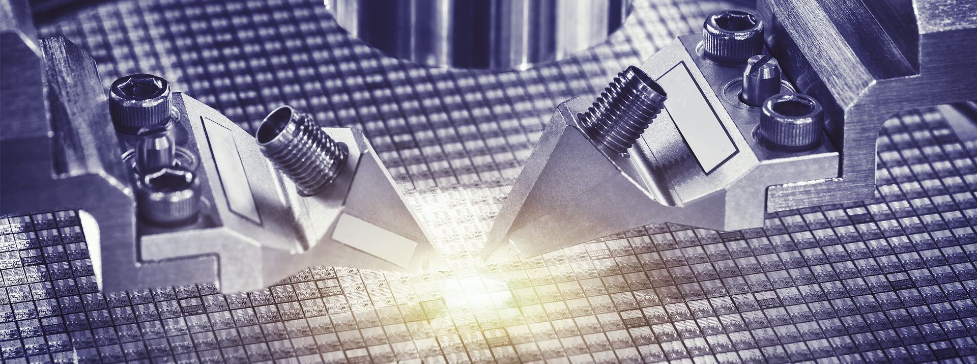
Manufacturing Optical Semiconductors - Processes and Quality Control -
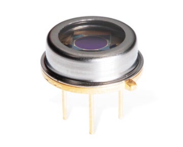
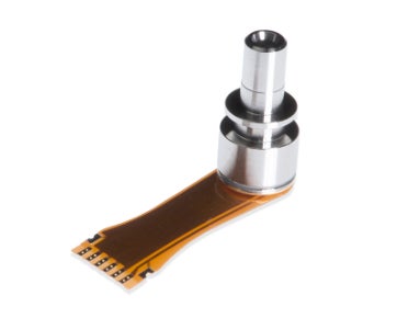
A light-receiving element that converts the intensity of incident light into an electric current
A photodiode is a light-sensitive device that converts the intensity of incident light into an electric current. The wavelength range and sensitivity it detects vary depending on the material used to construct the semiconductor device. When the material is silicon (Si), it is sensitive to wavelengths in the ultraviolet, visible light, and infrared (up to 1100 nm) ranges. When the material is a compound semiconductor such as InGaAs, it is sensitive to longer-wavelength infrared regions. By combining them with light sources, they can be used for various sensing applications.
InGaAs Photodiodes
Long-Wavelength InGaAs Photodiodes
Photovoltaic Power Converter
Electron-Cooled InGaAs Photodiode
Si Photodiodes
Si Photodiode Array
GaAs Photodiodes
Dual-Wavelength Photodiodes
GaN UV Sensors
Development of Waveguide-Type Photodiodes: Challenging High-Speed Performance Through Integration with UTC-PD

Photodiode (PD) Selection Guide: Comparison by Application and Optimal Selection Methods Read Article

Design Optimization and Latest Trends in Photodiodes (PD) for Communication Applications
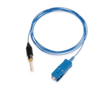
Optical Receiver Module
with Transimpedance Amplifier (TIA)
for Maximizing Avalanche Photodiode Performance
This optical receiver module features a transimpedance amplifier (TIA) to maximize the performance of avalanche photodiodes. It is suitable for optical communication products requiring long-distance transmission where the output of a PD-TIA alone is insufficient.
InGaAs PD-TIA Receiver
GaAs PD-TIA Receiver
What are Optical Semiconductor Devices?
Manufacturing Optical Semiconductors - Processes and Quality Control -
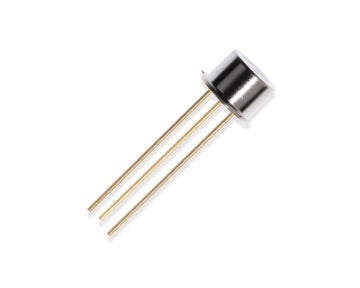
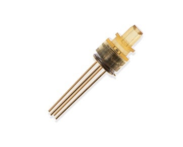
A semiconductor device that multiplies photoelectrons by applying a reverse bias voltage
An avalanche photodiode is a semiconductor device that multiplies photoelectrons by applying a reverse bias voltage. This multiplication enables the generation of a larger photocurrent compared to a photodiode. It is suitable for detecting faint light. We also offer APD modules capable of handling high reverse bias voltages.
KP-A InGaAs Avalanche Photodiodes
KP-A Si Avalanche Photodiodes
Manufacturing Optical Semiconductors - Processes and Quality Control -
Optical Receiver Module
with Transimpedance Amplifier (TIA)
Maximizing Avalanche Photodiode Performance
This optical receiver module features a transimpedance amplifier (TIA) to maximize the performance of the avalanche photodiode. It is suitable for optical communication products requiring long-distance transmission where the output of a PD-TIA alone is insufficient.
InGaAs APD-TIA Receivers
What are Optical Semiconductor Devices?
Manufacturing Optical Semiconductors - Processes and Quality Control -
A photodetector that amplifies the photocurrent generated
by a photodiode using a transistor before outputting the current
A phototransistor is a light-receiving element that integrates a photodiode and a transistor into a single structure. It amplifies the photocurrent generated by the photodiode using the transistor before outputting the current.
What are Optical Semiconductor Devices?
Manufacturing Optical Semiconductors - Processes and Quality Control -
Vertical-cavity surface-emitting laser
with the light-emitting section positioned on the top surface of the chip and emitting light vertically
VCSEL, Vertical Cavity Surface Emitting Laser, differs from conventional edge-emitting lasers in that its light-emitting region is located on the top surface of the chip and emits light vertically. We handle VCSELs with an emission wavelength band of 850 nm.
What are Optical Semiconductor Devices?
Manufacturing Optical Semiconductors - Processes and Quality Control -
SWIR Type Reflective Sensors for Medical Devices and Healthcare
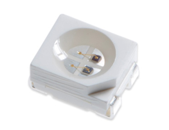
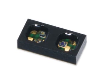
This reflective photo sensor features an LED chip (light-emitting element) and a photodiode chip (light-receiving element) mounted side-by-side within a single package. It performs sensing by directing the product toward the target object and utilizing reflected light. It can be used for detecting and analyzing various components, sensing different materials, and as a general-purpose photoelectric sensor or proximity sensor.
KPR SWIR Type Short-Wavelength Reflective Sensor
KPR SWIR Type Dual-Wavelength Reflective Sensor

Manufacturing of Optical Semiconductors: Processes and Quality Control

Fundamentals of Biometric Sensing Technology Using SWIR, Short-Wave Infrared

Technology Trends in Optical Sensors for Advancing Biometric Sensing Applications