Accelerating disruptive FPGA platform innovation
Efinix is an FPGA startup founded in the United States in 2012. Its revolutionary Quantum™ technology achieves four times the PPA (Power, Performance, Area) of conventional FPGAs. Trion FPGAs, leveraging this technology, are currently in mass production with low power consumption and optimal pricing, despite matching the performance of other FPGA manufacturers. Furthermore, Titanium FPGAs, which achieve even higher performance and integration, are also in mass production, with the product lineup being expanded sequentially.
The core technology of Efinix FPGAs is the innovative Quantum™ fabric, which offers advantages over traditional FPGA technology in power, performance, and area. Efinix Titanium FPGAs enable rapid time-to-market for innovation in the mainstream market, opening up new applications. With densities ranging from 4,000 to 1 million logic elements (LEs), Efinix FPGAs are ready to address your next design challenges, including custom logic, compute acceleration, and machine learning or deep learning.
Low Power, Small
Footprint,
Big Compute
The need is to pack as much computing power as possible into a space of just a few square millimeters.
Efinix's next-generation Titanium FPGA is manufactured using a 16nm process, delivering high performance with the lowest possible power consumption and smallest physical size.

The Titanium FPGA features an ultra-compact package measuring just 3.5mm x 3.4mm WLCSP and is designed for highly integrated applications.
Hardened MIPI D-PHY and DDR DRAM controllers support IoT, thermal cameras, industrial cameras, robotics, and smart devices.
Titanium devices monitor device integrity and can seamlessly and automatically recover from random SEU events, maximizing application uptime.
Bitstream authentication prevents unauthorized tampering, and bitstream encryption ensures design security.
Titanium products are designed for a wide range of applications across many diverse markets. Some of these markets are characterized by long product lifecycles, where once mass production begins, there is resistance to changes in bill of materials specifications or components. Efinix understands this and is committed to providing stable supply of supported products throughout your product lifecycle. We promise to support the Titanium family of FPGAs until at least 2045. For details on product lifecycles, please contact us.
*The table below can be swiped left and right.
| Features | Ti35 | Ti60 | Ti90 | Ti120 | Ti165 | Ti180 | Ti240 | Ti375 | Ti550 | Ti750 | Ti1000 |
|---|---|---|---|---|---|---|---|---|---|---|---|
| Logic Elements (LEs) |
36,176 | 62,016 | 92,534 | 123,379 | 162,800 | 176,256 | 236,888 | 370,137 | 550,000 | 750,000 | 1,000,004 |
| 10K Memory Blocks (Mb) | 1.53 | 2.62 | 6.88 | 9.18 | 12.1 | 13.11 | 17.62 | 27.53 | 40.92 | 55.8 | 74.4 |
| DSP Blocks | 93 | 160 | 336 | 448 | 590 | 640 | 860 | 1,344 | 2,006 | 2,736 | 3,648 |
| PLLs | 4 | 4 | 10 | 10 | 12 | 10 | 12 | 12 | 12 | 12 | 12 |
| GPIO | 34 | 34 | 80 | 80 | 181 | 80 | 181 | 181 | 200 | 200 | 200 |
| High-Speed I/O | 146 | 146 | 232 | 232 | 235 | 232 | 235 | 235 | 320 | 320 | 320 |
| LPDDR4/4x | — | — | x32 | x32 | 2x32 | x32 | 2x32 | 2x32 | 2x72 | 2x72 | 2x72 |
| MIPI D-PHY 2.5 Gbps | — | — | 4
RX 4 TX |
4
RX 4 TX |
3
RX 3 TX |
4
RX 4 TX |
3
RX 3 TX |
3
RX 3 TX |
3
RX 3 TX |
3
RX 3 TX |
3
RX 3 TX |
| Tranceivers | — | — | — | — | x16 | — | x16 | x16 | x24 | x24 | x24 |
| 25.8 Gbps Transceivers | — | — | — | — | — | — | — | — | x8 | x8 | x8 |
| Hardened RISC-V block | — | — | — | — |
Quad Core |
— |
Quad Core |
Quad Core |
Quad Core |
Quad Core |
Quad Core |
| PCIe® Gen4 (16G) | — | — | — | — | 2x4 | — | 2x4 | 2x4 | 2x8 | 2x8 | 2x8 |
*The table below can be swiped left and right.
| Package | Pitch (mm) |
Size (mm) |
Ti35 | Ti60 | Ti90 | Ti120 | Ti165 | Ti180 | Ti240 | Ti375 | Ti550 | Ti750 | Ti1000 |
|---|---|---|---|---|---|---|---|---|---|---|---|---|---|
| 64-ball WLCSP | 0.4 | 3.5x3.4 | |||||||||||
| 100-ball FBGA | 0.5 | 5.5x5.5 | |
||||||||||
| 225-ball FBGA | 0.65 | 10x10 | |
||||||||||
| 256-ball FBGA | 0.8 | 13x13 | |
||||||||||
| 361-ball FBGA | 0.65 | 13x13 | |
||||||||||
| 400-ball FBGA | 0.8 | 16x16 | |
||||||||||
| 484-ball FBGA | 0.8 | 18x18 | |
|
|
||||||||
| 529-ball FBGA | 0.8 | 19x19 | |||||||||||
| 676-ball FBGA | 0.8 | 22x22 | |
|
|||||||||
| 900-ball FBGA | 0.8 | 25x25 | |
|
|||||||||
| 1,156-ball FBGA | 1.0 | 35x35 | |
|
Low power consumption, high performance for mass production applications
A new family of devices ideal for mass production has arrived. Topaz FPGAs can be deployed at scale, combining a highly efficient architecture with commonly used features and protocols (PCIe Gen3, MIPI, LPDDR4, LVDS, etc.).
The Topaz architecture, designed to pack more logic into XLR cells, enables the implementation of more features.
Topaz FPGAs, equipped with commonly used protocols (LVDS, MIPI, Ethernet, PCIe Gen3), support applications such as machine vision, robotics, and printers.
Topaz FPGA offers a wide range of BGA packages that can be easily integrated into systems.
When you need to upgrade design performance or add logic, you can easily migrate from Topaz to Titanium FPGA.
Topaz products are designed for a wide range of applications across many diverse markets. Some of these markets are characterized by long product lifecycles, where once mass production begins, there is resistance to changes in bill of materials specifications or components. Efinix understands this and is committed to providing stable supply of supported products throughout your product lifecycle. We promise to support the Topaz family of FPGAs until at least 2045. For details on product lifecycles, please contact us.
*The table below can be swiped left and right.
| Features | Tz50 | Tz75 | Tz100 | Tz110 | Tz170 | Tz200 | Tz325 |
|---|---|---|---|---|---|---|---|
| Logic Elements (LEs) | 52,160 | 75,520 | 101,440 | 120,584 | 172,008 | 215,360 | 326,080 |
| 10K RAM blocks (Mb) | 2.4 | 5.34 | 6.32 | 6.41 | 11.14 | 15.77 | 19.22 |
| DSP blocks | 140 | 264 | 312 | 320 | 544 | 840 | 1008 |
| PLLs | 4 | 12 | 12 | 10 | 10 | 12 | 12 |
| GPIO | 34 | 133 | 133 | 80 | 80 | 181 | 181 |
| High-speed I/O | 146 | 139 | 139 | 232 | 232 | 235 | 235 |
| LPDDR4 | — | 1x32 | 1x32 | 1x32 | 2x32 | 2x32 | 2x32 |
| MIPI D-PHY 2 Gbps | — | 2 RX 2 TX |
2
RX 2 TX |
4
RX 4 TX |
4 RX 4 TX |
3 RX 3 TX |
3 RX 3 TX |
| 12.5 Gbps transceivers | — | x8 | x8 | — | — | x16 | x16 |
| Hardened RISC-V block | — | Quad Core |
Quad Core |
— | — | Quad Core |
Quad Core |
| PCIe® Gen3 (8G) | — | 1x4 | 1x4 | — | — | 2x4 | 2x4 |
*The table below can be swiped left and right.
| Package | Pitch (mm) |
Size (mm) |
Tz50 | Tz75 | Tz100 | Tz110 | Tz170 | Tz200 | Tz325 |
|---|---|---|---|---|---|---|---|---|---|
| 100-ball FBGA | 0.5 | 5.5x5.5 | |||||||
| 225-ball FBGA | 0.65 | 10x10 | |
||||||
| 256-ball FBGA | 0.8 | 13x13 | |
||||||
| 361-ball FBGA | 0.65 | 13x13 | |
|
|||||
| 400-ball FBGA | 0.8 | 16x16 | |||||||
| 400-ball FBGA | 0.5 | 10x10 | |
||||||
| 484-ball FBGA | 0.8 | 18x18 | |
|
|
|
|||
| 529-ball FBGA | 0.8 | 19x19 | |
|
|||||
| 576-ball FBGA | 0.65 | 16x16 | |||||||
| 676-ball FBGA | 0.8 | 22x22 | |||||||
| 676-ball FBGA | 0.65 | 18x18 | |
|
|||||
| 900-ball FBGA | 0.8 | 25x25 |
Realization of Advantages in the Power Performance Domain
This Trion® platform is manufactured using SMIC's 40nm LL process, offering logic density ranging from 4,000 to 120,000 logic elements (LE) and integrating standard interfaces such as GPIO, PLL, oscillators, MIPI, DDR, and LVDS. Trion FPGAs target the general-purpose custom logic market (mobile, IoT, general consumer products, industrial equipment, medical devices, etc.). They also support rapidly growing markets such as deep learning and compute accelerators in edge devices.

The Trion FPGA features the smallest package size of just 4.5mm x 3.6mm WLCSP and is designed for highly integrated applications.
The standard MIPI CSI-2 interface hardware controller supports IoT, thermal cameras, industrial cameras, robotics, and smart devices.
Processing data can be saved using the DDR DRAM hardware controller.
Trion products are designed for a wide range of applications across many diverse markets. Some of these markets are characterized by long product lifecycles, where once mass production begins, there is resistance to changes in bill of materials specifications or components. Efinix understands this and is committed to providing stable supply of supported products throughout your product lifecycle. We promise to support the Trion family of FPGAs until at least 2045. For details on product lifecycles, please contact us.
*The table below can be swiped left and right.
| Features | T4 | T8 | T13 | T20 | T35 | T55 | T85 | T120 |
|---|---|---|---|---|---|---|---|---|
| Logic Elements (LEs) | 3,888 | 7,384 | 12,828 | 19,728 | 31,680 | 54,195 | 84,096 | 112, 128 |
| Mask Programmable Memory (MPM) | — | — | — | — | ||||
| Internal Memory Bits (kb) | 77 | 123 | 727 | 1,044 | 1,475 | 2,765 | 4,055 | 5,407 |
| 18x18 Multipliers | 4 | 8 | 24 | 36 | 120 | 150 | 240 | 320 |
| PLLs | 1 | 5 | 5 | 7 | 7 | 8 | 8 | 8 |
| LVDS (TX, RX) | — | 6,6 | 13,13 | 20,26 | 20,26 | 52,52 | 52,52 | 52,52 |
| DDR3, LPDDR3, LPDDR2 (up to 1066 Mbps) | — | — | — | x16 | x16 | x32 | x32 | x32 |
| MIPI DPHY (4 lanes) with integrated MIPI CSI-2 controller | — | — | 2 RX 2 TX |
2 RX 2 TX |
2 RX 2 TX |
3 RX 3 TX |
3 RX 3 TX |
3 RX 3 TX |
*The table below can be swiped left and right.
| Package |
Pitch (mm) |
Size (mm) |
GPIO (1) |
PLLs |
SPI Flash (Mbit) |
LVDS Pairs TX,RX |
MIPI CSI-2 TX,RX(1) |
DDR DRAM(1) |
T4 | T8 | T13 | T20 | T35 | T55 | T85 | T120 |
|---|---|---|---|---|---|---|---|---|---|---|---|---|---|---|---|---|
| 49-ball FBGA | 0.4 | 3x3 | 33 | 1 |
|
|||||||||||
| 80-ball WLCSP | 0.4 | 4.5x3.6 | 33 | 3 | 1,1 |
|
||||||||||
| 81-ball FBGA | 0.5 | 5x5 | 55 | 1 |
|
|||||||||||
| 100-pin LQFP | 0.5 | 14x14 | 65 | 5 | 16 | 4,4 |
|
|
||||||||
| 144-pin LQFP | 0.5 | 20x20 | 97 | 5 | 6,6 |
|
||||||||||
| 169-ball FBGA | 0.65 | 9x9 | 73 | 5 | 8,12 | 2,2 |
|
|
||||||||
| 256-ball FBGA | 0.8 | 13x13 | 195 | 5 | 13,13 |
|
|
|||||||||
| 324-ball FBGA | 0.65 | 12x12 | 130 | 7 | 20,26 | 2,2 | x8,x16 |
|
|
|
|
|
||||
| 400-ball FBGA | 0.8 | 16x16 | 230 | 7 | 20,26 | x8,x16 |
|
|
||||||||
| 484-ball FBGA | 0.8 | 18x18 | 256 | 8 | 40,40 | x16,x32 |
|
|
|
|||||||
| 576-ball FBGA | 0.65 | 16x16 | 278 | 8 | 52,52 | 2,2 | x16,x32 |
|
|
|
(1) MIPI and DDR interfaces use dedicated I/O, so the maximum GPIO count does not include the I/O count for those interfaces.
Simple,Easy-to-Use Toolflow
Efinix®'s Efinity® provides a complete toolflow from RTL design to bitstream generation. It supports a simple, easy-to-use GUI interface and command-line scripting, and includes all the tools necessary for designing on Titanium and Trion® FPGAs.
Efinix provides Efinity software licenses free of charge. Additionally, purchasing a development kit includes a software license and one year of upgrades. After the initial year, you can request free maintenance updates. The version you receive supports all Efinix FPGAs, not the feature-limited Web Edition.
To obtain a free license, register at the Support Center on the official Efinix website. Next, click the Efinity page to request your free license. You will receive the license and one year of maintenance (upgrades and patches). You can request an additional year of maintenance free of charge at any time.
Efinity Software V2024.1 includes the following new features and enhancements:
Get started with the kit
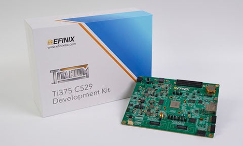
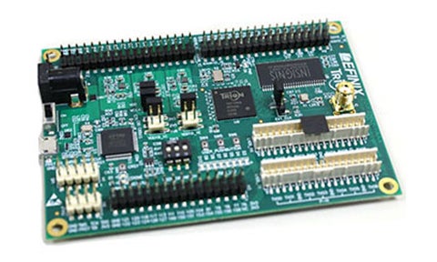
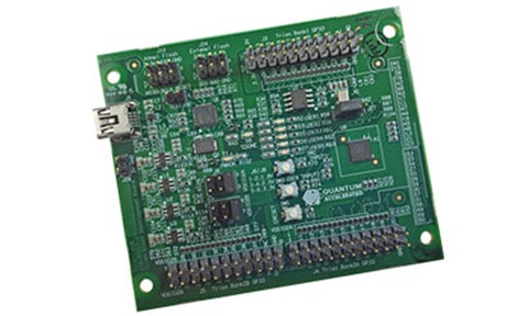
Efinix development kits help you quickly start designing with Efinix FPGAs. With each kit, you also receive a license for Efinity® software. Efinix offers several daughter cards separately, in addition to the card included in the kit.
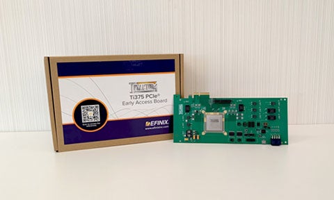
This early access board is Efinix's first board featuring the Ti375 FPGA and PCIe Gen4 x4 functionality. You can see the Ti375 PCIe transceivers in action.
This development kit enables you to develop applications for the Ti375 FPGA's hardened quad-core RISC-V processor, which can operate at clock frequencies up to 1 Gbps.
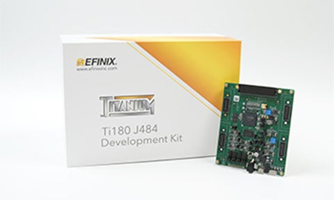
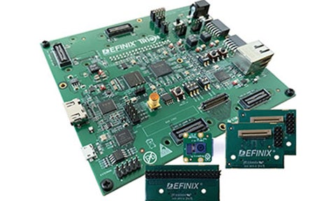
The Ti180 J484 Development Kit showcases the Ti180 FPGA's hardened MIPI D-PHY supporting up to 2.5 Gbps per lane and its hardened LPDDR4x controller.
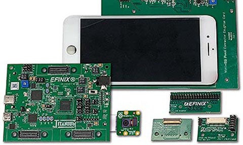
Everything needed for vision system prototyping is included: the Ti60 FPGA, Raspberry Pi camera, and DSI display.
Some Efinix Trion FPGAs feature a hardened MIPI CSI-2 block, providing excellent camera sensor interfaces and sufficient logic for image processing. The hard DDR DRAM memory controller can connect to frame buffers or other system memory. Efinix's MIPI CSI-2-based development kits connect to Raspberry Pi and other cameras, making it easy to prototype vision applications.
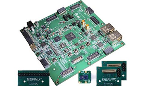
This T120 kit features a BGA576 package, offering more I/O, LPDDR3 memory, user inputs, and PMOD connectors, providing the functionality needed to create a complete system prototype.
Prototype designs using the T120 FPGA MIPI CSI-2 and DDR DRAM controllers. Process video and send it to a display via the HDMI connector, and connect custom peripherals using the PMOD connector.
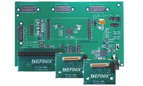
A starter MIPI CSI-2 development kit featuring the T20 FPGA. This kit includes three daughter cards that can connect to MIPI cameras and other external devices or extend GPIOs.
Efinix's I/O Expansion Kit provides access to I/O through connectors and headers on the board. These boards feature LEDs and switches, plus an additional clock oscillator on the board. They can be connected to other boards via headers and connectors or used standalone to demonstrate processing capabilities.
I/O breakout board featuring the T20 BGA256 FPGA
Starter board featuring the T8 BGA81 FPGA.
To deliver the best power, performance, and area (size) for silicon products, Efinix designed the Quantum® architecture, a leader in programmable technology. Our goal is to provide the most flexible programmable technology tailored for compute-intensive applications such as machine learning, deep learning, and high-speed computation accelerators.

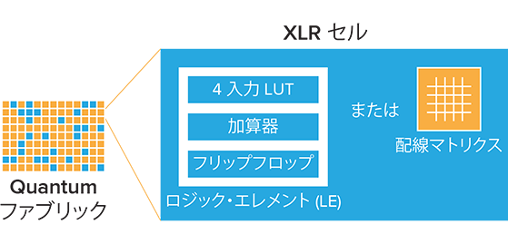
Switchable Logic and Routing (XLR) Cells
The fundamental building block of the Quantum® fabric is the switchable logic and routing (XLR) cell. The XLR cell functions as a LUT-based logic cell and as a routing switch transformed by a scalable and flexible routing structure. Software determines whether an XLR cell is logic or wiring. Having dedicated logic and dedicated wiring might seem like a good idea. However, most complex logic blocks have numerous input and output signals. Using all input and output signals would prevent access to the remaining logic within the block. Because any XLR cell can be used for wiring, software can avoid congestion and select the optimal path.
Advantages of XLR Cells
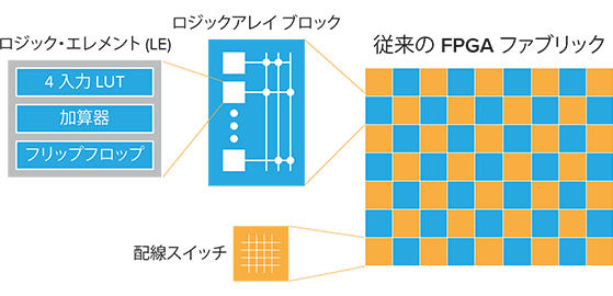
Comparison with traditional FPGAs and first-generation Quantum® fabric
Conventional FPGAs are designed with a fixed ratio of logic elements to wiring resources. This ratio is critical: insufficient wiring resources prevent proper connection of logic elements, leading to underutilization of the FPGA. Conversely, excessive wiring resources waste silicon area, increasing the chip cost.
Thanks to XLR cells, Efinix® FPGAs are smaller, consume less power, and are more efficient than traditional FPGAs. Unlike traditional FPGAs, Efinix® FPGAs are manufactured using standard CMOS silicon processes. Using standard processes makes our FPGAs easier to produce and optimizes high-volume manufacturing.
Level Up with Quantum® Computing Fabric
The second-generation Quantum® Computing Fabric incorporates high-efficiency XLR cells, along with 10K memory blocks and high-performance DSP blocks, to enable even greater computational processing and flexible interconnectivity.
The Quantum computing architecture consists of configurable tiles, switchable logic, and interconnect (XLR) cells, optimizing interconnect efficiency and speed while achieving high utilization. This architecture also incorporates highly configurable embedded memory blocks and dedicated high-speed DSP blocks. Combining these features delivers optimal performance for a wide range of applications, from edge computing to industrial automation and video processing.
Efinix FPGA configuration modes are broadly categorized into the following three types.
Configuration Mode
| Mode | Description |
|---|---|
| SPI Active | Mode where the FPGA acts as the SPI Master. An external SPI Flash is connected, and the FPGA reads the bitstream via SPI communication for configuration. |
| SPI Passive | Mode where the FPGA acts as an SPI Slave. Configuration occurs by streaming the bitstream from an external SPI Master device, such as a microcontroller, into the FPGA. |
| JTAG | Configuration occurs by streaming the bitstream from a host computer or similar device into the JTAG interface. Primarily used during debugging. |